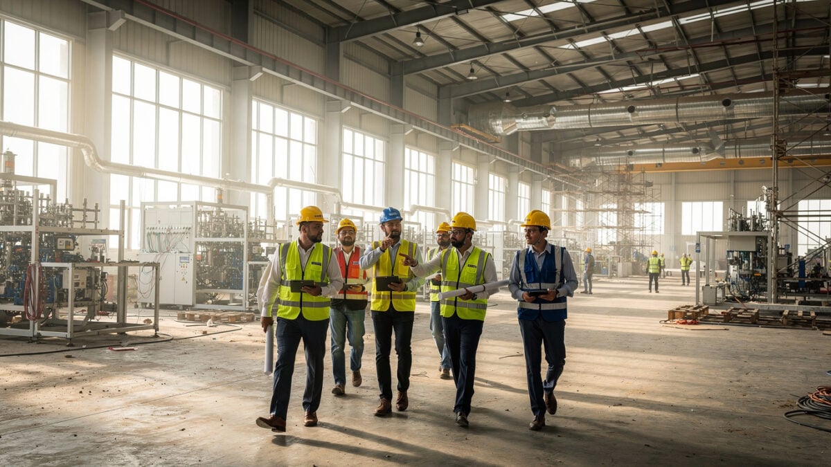
India launched the second phase of its semiconductor mission, Semicon 2.0, with a government outlay of Rs 1,27,500 crore — roughly $13.5 billion — at the Semicon India 2026 conference in New Delhi on September 17, 2026. U.S. equipment makers Applied Materials and Lam Research pledged $5 billion and approximately Rs 10,000 crore, respectively, for research, supply-chain capacity, and a first silicon-component manufacturing facility.
The announcements sit inside a $30 billion investment pitch. How much of that figure is binding private capital, and how much is policy ceiling and aspirational pipeline, remains opaque.
The $30 billion figure arrived at the Semicon India conference wrapped in the language of national ambition. Strip away the conference-stage signaling and the number is harder to pin down. It blends a government outlay of Rs 1,27,500 crore — approved by the Union Cabinet on July 15, 2026 — with multi-billion-dollar pledges from two U.S. equipment makers and a pipeline of projects that have not yet cleared the cabinet. The headline suggests unified backing. The breakdown suggests something closer to a policy ceiling with private commitments still taking shape.
Prime Minister Narendra Modi told the gathering that the world urgently needs new and reliable manufacturing locations. Modi said India is readying itself for that role. The question the conference left unanswered is how much of the capital on display is ready to be deployed, and how much is still a bet on guidelines that have not been written.
The pledges that give the number weight
Applied Materials committed $5 billion over the next decade. The plan includes a 140-acre research park and a push to deepen supply-chain capacity and workforce development in India. Prabhu Raja, who runs the company’s semiconductor products group, framed it as a long-term bet: “Inventions done here must scale globally.”
Lam Research said it would invest approximately Rs 10,000 crore to build its first silicon component manufacturing facility in the country. Sesha Varadarajan, the company’s chief operating officer, confirmed the figure on the conference sidelines.
The government’s own commitment is now codified. The Union Cabinet approved Semicon 2.0 on July 15, 2026, with a total outlay of Rs 1,27,500 crore, according to the Press Information Bureau. The programme’s first phase, launched in December 2021, had an outlay of Rs 76,000 crore. The second phase runs for 12 years and shifts the focus from broad ecosystem buildout toward equipment, materials, advanced packaging, and talent.
Union Minister Ashwini Vaishnaw said Semicon 2.0 would target at least 200 chip-design startups. Ashok Chandak, president of SEMI India, projected that the sector could attract cumulative private and industry investments of around Rs 5-6 lakh crore over the next five to seven years. More than 600 companies and representatives from 52 countries attended the conference, signaling the breadth of interest.
But the $30 billion figure that framed the conference is not a single number with a single owner. It is a composite of government outlays, announced private pledges, and a pipeline of projects that have not yet cleared the cabinet. The government’s own press release does not break out how much is binding.
The number is doing political work
India’s semiconductor sector had drawn $1.4 billion in all-time equity funding across 281 funded companies as of mid-September 2026, according to Tracxn-based data. That includes $228 million raised this year. The figures show capital formation is improving, but it remains concentrated well below the scale of the headline $30 billion pitch.
By July 15, 2026, India had approved 12 manufacturing units under its semiconductor incentive plans, according to Reuters. Semicon 2.0 is designed to deepen capabilities in equipment, materials, IP, and supply chains. The policy is a long-duration buildout, not an immediate capacity boom. Operational guidelines that will set subsidy rates and eligibility are expected in the weeks ahead. If they appear, pledges can begin converting into bankable projects. If they do not, the gap between headline numbers and funded capacity will widen.
India is not trying to win the leading-edge chip race first. Taiwan remains ahead in fabrication, South Korea leads in memory, and the United States dominates design and equipment. India is entering through assembly, packaging, and mature-node manufacturing, where it has policy momentum but still lacks a proven large-scale fab record. China remains the deepest rival in scale, while Vietnam and Malaysia compete in back-end manufacturing and supply-chain diversification.
The $30 billion figure is doing political work, not capital-allocation work. Until the operational guidelines translate pledges into bankable projects, the number will remain a ceiling, not a floor.
Beyond the headline
The money trail
The real money is flowing into the tools and inputs layer, not just future fabs. Equipment makers can monetize India before a single large fabrication plant reaches steady output. That shifts the story from one of national ambition to one of supplier-led positioning.
The bigger picture
India is not trying to win the leading-edge chip race first. It is building a defensible position in the parts of the supply chain that are easier to localize. The benchmark moves from headline megafab announcements to whether packaging, materials, and engineering talent can compound into an ecosystem.
What isn’t being said
The missing question is how much of the $30 billion number is actually committed capital versus policy ceiling and aspirational pipeline. Without that split, the headline can overstate certainty. Public support is real, but the mix of binding private investment, conditional expansion plans, and conference-stage signaling is still opaque.
The capital is real, the timeline is not
With Semicon 2.0 now approved and equipment-maker pledges on the table, the next six months will determine whether the $30 billion figure hardens into deployed capital or remains a policy target.
- Western semiconductor equipment procurement manager
Review the updated India Semiconductor Mission and MeitY program pages over the next 30 days for the final subsidy structure and eligibility rules. The commitments from Applied Materials and Lam Research signal near-term demand for tools and materials; identify sales channels tied to their India buildout plans.
- US-based investor with APAC emerging market exposure
Track quarterly India revenue updates from Applied Materials and Lam Research in their next two earnings cycles. The conversion of pledges into orders will show whether the India capex story is accelerating. Supplier names with direct exposure to the equipment and materials layer offer a clearer entry point than pure-play fab bets.
- Western electronics supply chain strategist
Analyze the specifics of India’s semiconductor ecosystem development, including the talent pool and infrastructure, to assess its viability for future supply chain diversification. The 140-acre research park and Lam Research’s silicon-component facility are concrete signals, but the absence of a large-scale fab track record means near-term diversification will be in packaging and testing, not leading-edge production.
- Western government policy advisor on Indo-Pacific trade
Assess the implications of India’s semiconductor growth on existing trade agreements, technology transfer policies, and geopolitical strategies. The expansion gives U.S. equipment makers a second growth channel while China exposure remains sensitive, adding an India dimension to export controls and supply-chain diplomacy.
Explainer
- Semicon 2.0
- The second phase of India’s semiconductor programme, approved by the Union Cabinet on July 15, 2026, with a total outlay of Rs 1,27,500 crore. It shifts focus from broad ecosystem creation to equipment, materials, advanced packaging, research, and talent development. The programme runs for 12 years and builds on the first phase launched in December 2021.
- India Semiconductor Mission
- The overarching government initiative to develop a complete semiconductor ecosystem in India, from design to fabrication, assembly, testing, and packaging. Launched in January 2022, it has approved 12 manufacturing projects and entered into cooperation agreements with the United States, Japan, the European Union, Singapore, and the Netherlands.
- NITI Aayog
- The Indian government’s premier policy think tank, formally the National Institution for Transforming India. It released India’s first comprehensive 10-year semiconductor roadmap in May 2026, targeting a $120–150 billion semiconductor value chain by 2035. The roadmap emphasizes advanced packaging, compound semiconductors, and AI-native chip design.
RELATED STORIES