Nvidia announced a $1.5 billion prepayment to Amkor Technology on 23 July, securing advanced chip packaging capacity at a future Arizona plant. Amkor shares jumped roughly 12% in after‑hours trading.
The facility won’t begin volume production until early 2028, meaning the bet addresses a bottleneck that has repeatedly constrained Nvidia’s AI accelerator shipments—but not immediately.
Nvidia is wiring Amkor Technology $1.5 billion to lock in advanced chip packaging capacity—a production step that has turned into the narrowest point in the AI hardware pipeline. The payment, structured as a prepayment rather than an equity stake, guarantees future access to assembly and test services without diluting the chip designer’s balance sheet.
The campus that will fill those orders, a $7 billion total investment across two phases in Peoria, Arizona, won’t begin volume production until early 2028. That timeline did not stop investors from pushing Amkor’s shares up roughly 12% in extended trading on 23 July. The reaction signals a willingness to price in a supply‑chain fix that remains years away—and a conviction that Nvidia is building something more durable than a short‑term capacity grab.
The prepayment that rewrites a capex plan
Amkor’s Peoria campus is a two‑phase project with an expected total cost of about $7 billion. The first manufacturing building is scheduled for completion by mid‑2027, with high‑volume packaging ramp‑up targeted for early 2028. Nvidia’s $1.5 billion commitment is significant by any measure: it equals roughly 50% to 60% of the packager’s entire 2026 capital‑expenditure guidance of $2.5 billion to $3.0 billion.
The prepayment effectively underwrites the risky expansion, letting Amkor order equipment and break ground with a locked‑in anchor customer. The US Department of Commerce has proposed up to $400 million in direct CHIPS and Science Act funding for the site, explicitly tied to building domestic 2.5D and 3D packaging capabilities. That public subsidy combines with Nvidia’s private cheque to accelerate a facility that would otherwise take far longer to justify financially.
The deal extends a pattern: Nvidia has been using its balance sheet to secure multiple supply‑chain nodes. A warrant‑backed arrangement with Corning locked in US manufacturing capacity, while a separate commitment secured SK Hynix for next‑generation HBM4 memory. The Amkor prepayment adds the most constrained step of all to that portfolio.
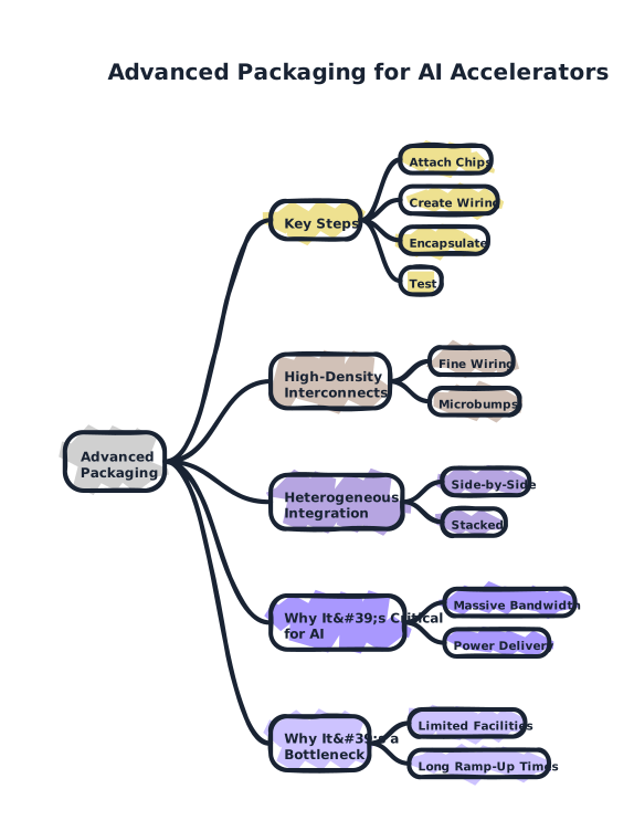
The assembly steps that turn bare silicon into an AI brain are easier seen than described.
| Entity | Current rule | New rule | Effective date |
|---|---|---|---|
| Amkor Peoria campus | No dedicated federal funding for advanced packaging | Up to $400 million CHIPS Act grant for 2.5D and 3D packaging | Announced; finalisation pending |
| Amkor (via CHIPS conditions) | No restrictions on expansion abroad | New investments in countries of concern restricted; workforce and community benefits required | Upon grant agreement |
| Other US‑based OSATs | Must shoulder expansion costs alone | Eligible for CHIPS funding if they meet national‑security thresholds | Rolling application windows |
| Source: US Department of Commerce CHIPS Program Office, Amkor disclosures | |||
The two companies will also collaborate on packaging technologies for next‑generation AI platforms, focusing on high‑density interconnect and heterogeneous integration—placing compute, memory and networking dies in a single package. “Amkor’s capabilities and US investment are critical to resilient AI infrastructure,” said Debora Shoquist, Nvidia’s executive vice‑president of operations.
Neither firm disclosed how much additional packaging volume the prepayment will yield, nor a precise production start date. That leaves the near‑term bottleneck unresolved: TSMC’s CoWoS lines remain the primary constraint on AI accelerator shipments through at least 2027.
Building a US packaging ecosystem, one cheque at a time
Nvidia’s move elevates Amkor from a long‑standing partner into the Western counterweight to TSMC’s Asian packaging dominance. Global advanced packaging is controlled by TSMC and Samsung, which offer CoWoS and similar technologies tightly integrated with their leading‑edge fabs. Independent OSATs like ASE, Amkor and JCET compete for the remaining work, but none has the same scale. On US soil, Intel‘s in‑house Foveros and EMIB solutions exist, yet Amkor’s neutral‑provider model means it can serve Nvidia, AMD and others simultaneously.
Amkor already packages chips for AMD, and in June it signed a 10‑year advanced packaging agreement with TSMC, positioning its Arizona site as a natural complement to the foundry’s nearby fabs. That multi‑customer design is the structural difference from Asia’s captive packaging lines. It gives Western chip designers a domestic alternative that reduces single‑region risk while keeping competitive pressure on TSMC‑linked capacity.
Nvidia is not acting alone. Asia’s smartest money is already betting that the AI build‑out’s real value lies in hard manufacturing assets. The prepayment to Amkor fits that pattern—backing a physical plant rather than a software layer. The next test arrives on 27 July, when Amkor reports earnings. If management quantifies the targeted packaging volumes and the Arizona build schedule, investors can begin modelling real supply relief. If the details remain vague, the market’s 12% surge will look as anticipatory as the factory’s 2028 timeline.
The company that designs the world’s most advanced AI chips is now underwriting the factory that will package them—not in Taiwan, but in Arizona. The share price didn’t jump on next‑quarter deliveries; it re‑rated on a bet about where the next decade of AI hardware will be built.
Beyond the headline
The Bigger Picture
Nvidia’s prepayment is part of a quiet restructuring of the AI hardware stack. Control over back‑end packaging is becoming as strategic as access to advanced wafers. By anchoring a second packaging source in the US, Nvidia is helping turn geographically concentrated bottlenecks into a more distributed network. That shift underpins not just chip supply but where future AI data‑centre investments and jobs will cluster.
The Money Trail
While $1.5 billion is small relative to Nvidia’s AI revenue, it is large against Amkor’s annual capex, effectively underwriting a risky multibillion‑dollar Arizona campus. Public subsidies via CHIPS funding reduce Amkor’s financing burden, but Nvidia’s named commitment is what convinces investors the capacity will be used. The cash flows will ultimately depend on long‑term utilisation—whether Nvidia and peers keep funnelling high‑margin AI packages through this US site.
The Timing
This agreement lands as CHIPS awards accelerate and TSMC’s Arizona fabs move closer to production, creating a narrow window to lock in complementary packaging capacity. At the same time, AI server demand remains constrained by CoWoS bottlenecks, making capacity reservations particularly valuable now. Signing a long‑term deal before the Peoria campus is built allows Nvidia to shape the facility’s design around its next‑generation platforms rather than retrofitting later.
The decisions ahead for four corners of the chip economy
The prepayment commits Nvidia to a future supply that won’t materialise for at least 18 months, leaving different audiences with distinct near‑ and medium‑term choices.
- US‑based semiconductor supply chain manager
You can now begin modelling a second advanced packaging source outside Asia. Monitor Amkor’s quarterly capex updates and the US Department of Commerce’s CHIPS funding portal for construction milestones. The Arizona site will not ease lead times this year, but it will alter your 2028 sourcing strategies and geographic risk assessments.
- Investor with exposure to semiconductor manufacturing stocks
Re‑evaluate OSATs with US‑based advanced packaging assets. Amkor’s multi‑customer model and Nvidia’s anchor commitment could lift its valuation multiple over Asian peers. Track the 27 July earnings call for volume targets; without them, the 12% share surge may prove premature.
- US government official overseeing CHIPS Act implementation
The Amkor‑Nvidia deal validates the Act’s back‑end packaging incentives. Publicly tying the $400 million grant to specific 2.5D and 3D capacity milestones and workforce plans will demonstrate a return on federal investment and inform future funding rounds for similar projects.
- AI cloud service provider procurement lead
Near‑term GPU availability will continue to depend on TSMC’s CoWoS lines. Use Nvidia’s quarterly data‑centre guidance to gauge when packaging constraints begin to loosen, but plan infrastructure scaling around 2028 for any realistic uplift from the Arizona plant. Negotiate multi‑year commitments that reflect a bifurcated supply timeline.
FAQ
Will this deal shorten AI server lead times soon?
No immediate relief is expected. Amkor’s Peoria campus won’t begin volume production until early 2028, and TSMC’s CoWoS lines remain the primary near‑term bottleneck. Enterprise buyers should anticipate that availability will still depend on existing Asian packaging capacity through at least 2027, with the US‑anchored second source influencing medium‑term delivery schedules instead.
Will Nvidia’s accelerators get cheaper?
The deal targets capacity and supply resilience rather than price cuts. US‑based packaging may carry higher operating costs than some Asian sites, and GPU pricing will continue to reflect wafer costs, memory pricing and demand intensity. Additional capacity could eventually dampen extreme premiums, but not during the initial ramp years.
Will the Peoria site serve other chip designers?
Yes. Amkor has indicated its Arizona campus is designed as a multi‑customer hub. It already packages chips for AMD and has a 10‑year US packaging agreement with TSMC, suggesting wafers from TSMC’s Arizona fabs and other designers could be processed there. However, no specific capacity split among customers has been publicly detailed.
Explainer
- Advanced packaging
- The stage where bare silicon dies are combined with memory and interconnects into a single module ready for server installation. Techniques like 2.5D and 3D integration stack or place chips side‑by‑side, relying on dense microscopic wiring on an interposer. Its complexity has made it the tightest step in AI chip production.
- CoWoS
- TSMC’s Chip‑on‑Wafer‑on‑Substrate technology, the dominant method for packaging high‑end AI accelerators. It places logic and memory dies on a silicon interposer, then bonds them to a substrate. Nvidia’s reliance on CoWoS has been the primary bottleneck limiting GPU shipments.
- OSAT
- Outsourced Semiconductor Assembly and Test provider. These companies package and test chips for fabless designers. Amkor, ASE and JCET are leading OSATs, competing to serve AI and high‑performance computing customers without owning wafer fabs themselves.
- Heterogeneous integration
- Combining different chip types—compute, memory, networking—into a single package so they operate as one system. High‑density interconnects and advanced packaging enable this integration, which is essential for AI accelerators that require massive bandwidth and tight physical proximity between logic and memory.
- CHIPS and Science Act
- A 2022 US law providing $52 billion to boost domestic semiconductor manufacturing and research. It includes grants for advanced packaging like Amkor’s Peoria project and imposes conditions on recipients, such as workforce benefits and restrictions on certain overseas investments.
RELATED STORIES